


Texas Instruments Texas Instruments CDCE(L)949 4-PLL VCXO-Taktsynthesizer
Der Texas Instruments CDCE(L)949 4-PLL VCXO-Taktsynthesizer sind modulare, kostengünstige, PLL-basierte, programmierbare Hochleistungs-Taktsynthesizer, Vervielfacher und Teiler. Dieses Gerät generiert aus einer einzigen Eingangsfrequenz bis zu 9 Ausgangstakte. Jeder Ausgang kann systemintern mit Einsatz von bis zu vier unabhängig konfigurierbaren PLLs für Taktfrequenzen bis zu 230MHz konfiguriert werden. Der CDCE(L)949 verfügt über separate Ausgangsversorgungs-Pins, VDDOUT, von 2,5V bis 3,3V. Der Eingang akzeptiert ein externes Quarz oder ein LVCMOS-Taktsignal. Wenn ein externer Quarz verwendet wird, genügt ein On-Chip-Lastkondensator für die meisten Anwendungen. Der Wert des Lastkondensators ist von 0 bis 20pF programmierbar. Zusätzlich ist ein On-Chip-VCXO wählbar, der die Synchronisierung der Ausgangsfrequenz mit einem externen Steuersignal, einem PWM-Signal, ermöglicht.
The CDCE(L)949 has separate output supply pins, VDDOUT, of 2.5V to 3.3V. The input accepts an external crystal or LVCMOS clock signal. If an external crystal is used, an on-chip load capacitor is adequate for most applications. The value of the load capacitor is programmable from 0 to 20pF. Additionally, an on-chip VCXO is selectable, allowing synchronization of the output frequency to an external control signal, that is, a PWM signal.
Merkmale
- Member of programmable clock generator family
- CDCE913/CDCEL913: 1 PLLs, 3 outputs
- CDCE925/CDCEL925: 2 PLLs, 5 outputs
- CDCE937/CDCEL937: 3 PLLs, 7 outputs
- CDCE949/CDCEL949: 4 PLLs, 9 outputs
- In-system programmability and EEPROM
- Serial programmable volatile register
- Non-volatile EEPROM to store customer settings
- Highly flexible clock driver
- Three user-definable control inputs (S0/S1/S2) e.g. SSC-selection, frequency switching, output enable or power down
- Generates highly-accurate clocks for video, audio, USB, IEEE1394, RFID, generates common clock frequencies used with TI DaVinci™, OMAP™, and DSPs
- BlueTooth™, WLAN, Ethernet, and GPS
- Programmable SSC modulation
- Enables 0-PPM clock generation
- Selectable output frequency up to 230MHz
- Flexible input clocking concept
- 8MHz to 32MHz external crystal
- On-chip VCXO: pull-range ±150ppm
- Single-ended LVCMOS up to 160MHz
- Low-noise PLL core
- Integrated PLL loop filter components
- Very low period jitter (60ps typical)
- Separate output supply pins
- CDCE949: 3.3V and 2.5V
- CDCEL949: 1.8V
- 1.8V device power supply
- Wide -40°C to +85°C temperature range
- Packaged in TSSOP
- Development and programming kit for easy PLL design and programming (TI-Pro clock)
Applikationen
- D-TV, HD-TV, STB, IP-STB, DVD-Player, DVD-Recorder, and Printer
- General-purpose frequency synthesizing
Datasheets
Functional Block Diagram
949_blkdia.png "Blockdiagramm - Texas Instruments Texas Instruments CDCE(L)949 4-PLL VCXO-Taktsynthesizer")
Development Tools

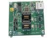
Texas Instruments CDCE949PERF-EVM Evaluationsmodul
Überprüft die Funktionalität und Leistungsfähigkeit des CDCE949 VCXO-Takt-Synthesizers.
Texas Instruments Texas Instruments CDCEL9XXPROGEVM Familie EEPROM-Programmierplatine
Ermöglicht eine schnelle Programmierung von Prototyp-Mustern oder kleinen Stückzahlen der CDCE(L)-Familie.
Veröffentlichungsdatum: 2016-01-06
| Aktualisiert: 2022-03-11