Everspin Technologies EMxxLX MRAM Memory Devices
Everspin EMxxLX MRAM Memory Devices are Expanded Serial Peripheral Interface (xSPI) based on a unique industrial STT MRAM technology. These memory devices are high-performance, multiple I/O, and SPI-compatible Magnetoresistive Random Access memory (MRAM) devices. The EMxxLX memory devices feature a high-speed, low pin count SPI-compatible bus interface with a clock frequency of up to 200MHz. These memory devices also feature a 1.65V to 2V voltage range, a dedicated 256-byte OTP area outside main memory, 3-byte and 4-byte address modes, and low power modes. Typical applications include industrial automation, datacenter, engineering emulation, automotive and transportation, and gaming.Features
- Expanded SPIbus interface supporting Octal, Quad, Dual, and single SPI protocol
- Up to 200MHz Single- and Double Transfer Rate (STR/DTR) for Octal SPI
- Up to 133MHz, SPI, DSPI, and QSPI
- Unlimited read, write, and erase operations for the supported life of the product
- 10 years minimum data retention across temperature
- JEDEC compliant: JESD251 and JESD251-1
- Byte-level writes and reads with no erase required as persistent memory
- Data integrity with no external ECC required
- Low power modes:
- <350μA (64Mb) standby
- Deep power down ∼50μA w/ exit time <100μs
- SPI compatibility: NVSRAM, FRAM, NOR, and toggle MRAM
- SPI, xSPI commands for program/erase emulated NOR compatible Execute-in-place (XIP)
- Nonvolatile settings are not reflow-protected
- Dedicated 256-byte OTP area outside main memory:
- Readable and user-lockable
- Permanent lock with WRITE OTP command
- Not reflow protected
- Erase capability:
- Chip/bulk erase and sector erase
- Subsector erase 4KB, 32KB granularity
- Security and writing protection:
- 16 configurable hardware write-protected regions plus top/bottom select
- Program/erase protection during power-up
- CRC command to detect accidental changes to user data
- 1.65V to 2V (1.8V) voltage range
- Density:
- 8Mb, 16Mb, 32Mb, and 64Mb
- 400MBps sustained throughput with OSPI at 200MHz, DTR, for reads and writes
- Boot mode configurations in x1, x2, x4, and x8
- Software reset and hardware reset pins available
- 3-byte and 4-byte address modes
- Sequential (burst) reads and writes
- JEDEC-standard 3-byte signature
- JEDEC standard, RoHS compliant packages:
- 24-ball BGA, 6mm x 8mm (5 x 5 array)
- 8-pin DFN, 6mm x 8mm
- Operating temperature ranges:
- Commercial from 0°C to +70°C
- Industrial from -40°C to +85°C
Applications
- Industrial automation
- Data center
- Engineering emulation
- Automotive and transportation
- Gaming
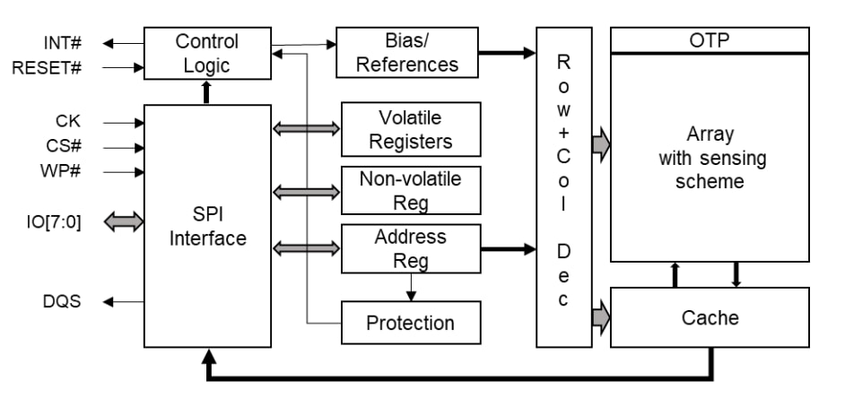
Block Diagram

Veröffentlichungsdatum: 2022-11-30
| Aktualisiert: 2025-09-15


