


Analog Devices Inc. AD5691, AD5692, & AD5693 nanoDAC+ DACs
Die ADI AD5691R, AD5692R & AD5693R nanoDAC+® Digital-Analog-Wandler sind 16-/14-/12-Bit gepufferte Spannungsausgangs-DACs mit niedrigem Stromverbrauch und Einzelkanal. Die Geräte enthalten eine standardmäßig aktivierte 2,5V-Referenz, die 2ppm/°C Drift bietet. Die Ausgangsspanne kann auf zwischen 0V bis VREF oder 0V bis 2 × VREF programmiert werden. Alle Geräte können über eine einzelne 2,7V bis 5,5V-Versorgung betrieben werden und sind durch die Konstruktion garantiert monoton. Die Geräte sind in LFCSP-Gehäusen von 2,00mm × 2,00mm mit 8 Anschlüssen oder in MSOP-Gehäusen mit 10 Anschlüssen erhältlich. Der interne Power-on-Reset-Schaltkreis gewährleistet, dass das DAC-Register beim Einschalten in Null-Skala geschrieben wird, während der interne Ausgangspuffer im Normalmodus konfiguriert ist. Die AD5693R/AD5692R/AD5691R enthalten einen Abschaltmodus, der den Stromverbrauch des Geräts auf 2μA (Maximum) bei 5V senkt und der eine über die Software auswählbare Ausgangsbelastungen bietet. Die AD5693R/AD5692R/AD5691R nutzen eine I2C-Schnittstelle. Einige Geräteoptionen enthalten außerdem einen asynchronen RESET-Kontakt und einen VLOGIC-Kontakt, die eine 1,8V-Kompatibilität zulassen.
The devices are available in a 2.00mm × 2.00mm, 8-lead LFCSP or a 10-lead MSOP. The internal power-on reset circuit ensures that the DAC register is written to zero scale at power-up while the internal output buffer is configured in normal mode. The AD5693R/AD5692R/AD5691R contain a power-down mode that reduces the current consumption of the device to 2μA (maximum) at 5V and provides software selectable output loads. The AD5693R/AD5692R/AD5691R use an I2C interface. Some device options also include an asynchronous RESET pin and a VLOGIC pin, allowing 1.8 V compatibility.
Merkmale
- 2mm × 2mm, 8-lead LFCSP Ultra-small package
- ±2LSB maximum at 16 bits High relative accuracy (INL)
- 2ppm/°C typical Low drift, 2.5V reference
- 2.5V or 5V Selectable span output
- ±0.06% of FSR maximum Total unadjusted error (TUE)
- ±1.5mV Maximum offset error
- ±0.05% of FSR maximum Gain error
- 0.1nV-sec Low glitch
- 20mA High drive capability
- 1.2mW at 3.3V Low power
- 1.8V to 5.5V Independent logic supply
- −40°C to +105°C Wide operating temperature range
- Robust 4kV HBM ESD protection
Applikationen
- Process controls
- Data acquisition systems
- Digital gain and offset adjustment
- Programmable voltage sources
- Optical modules
Block Diagram

Related Products

Analog Devices Inc. AD5693 16-Bit nanoDAC+
Winziger, energiesparender 16-Bit Einzelkanal-DAC mit gepuffertem Spannungsausgang mit ±2 (16-Bit) LSB INL.
DEVELOPMENT TOOLS
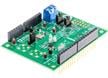
Analog Devices Inc. EVAL-AD5693RARDZ Evaluierungsboard
Ermöglicht ein schnelles Prototyping von AD5693R- Schaltungen und verkürzt die Entwicklungszeit.