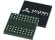
AS4C64M16D2A-25BIN

Bilder dienen lediglich der Veranschaulichung und sind nicht Originalgetreu
Siehe Produktspezifikationen
Siehe Produktspezifikationen
913-4C64M16D2A25BIN
AS4C64M16D2A-25BIN
Herst.:
Beschreibung:
DRAM DDR2, 1G, 64M x 16, 1.8V, 96-ball BGA, 400 MHz, (A-die), Industrial Temp - Tray
DRAM DDR2, 1G, 64M x 16, 1.8V, 96-ball BGA, 400 MHz, (A-die), Industrial Temp - Tray
Datenblatt:
Verfügbarkeit
-
Lagerbestand:
-
0Ein unerwarteter Fehler ist aufgetreten. Bitte versuchen Sie es später noch einmal.
-
Auf Bestellung:
-
418erwartet ab 02.06.2026
-
Lieferzeit ab Hersteller:
-
8Wochen Geschätzte Produktionszeit des Werks für Mengen, die größer als angezeigt sind.
Preis (CHF)
| Menge | Stückpreis |
Erw. Preis
|
|---|---|---|
| 12.76 CHF | 12.76 CHF | |
| 11.83 CHF | 118.30 CHF | |
| 11.46 CHF | 286.50 CHF | |
| 10.92 CHF | 546.00 CHF | |
| 10.65 CHF | 1 065.00 CHF | |
| 10.49 CHF | 2 192.41 CHF | |
| 10.22 CHF | 4 271.96 CHF |
Datenblatt
Konformitätscodes
- CNHTS:
- 8542319090
- CAHTS:
- 8542320020
- USHTS:
- 8542320032
- MXHTS:
- 8542320201
- ECCN:
- EAR99
Ursprungsklassifikationen
- Ursprungsland:
- Taiwan
- Herstellungsland:
- Taiwan
- Land der Verbreitung:
- Taiwan